The short version
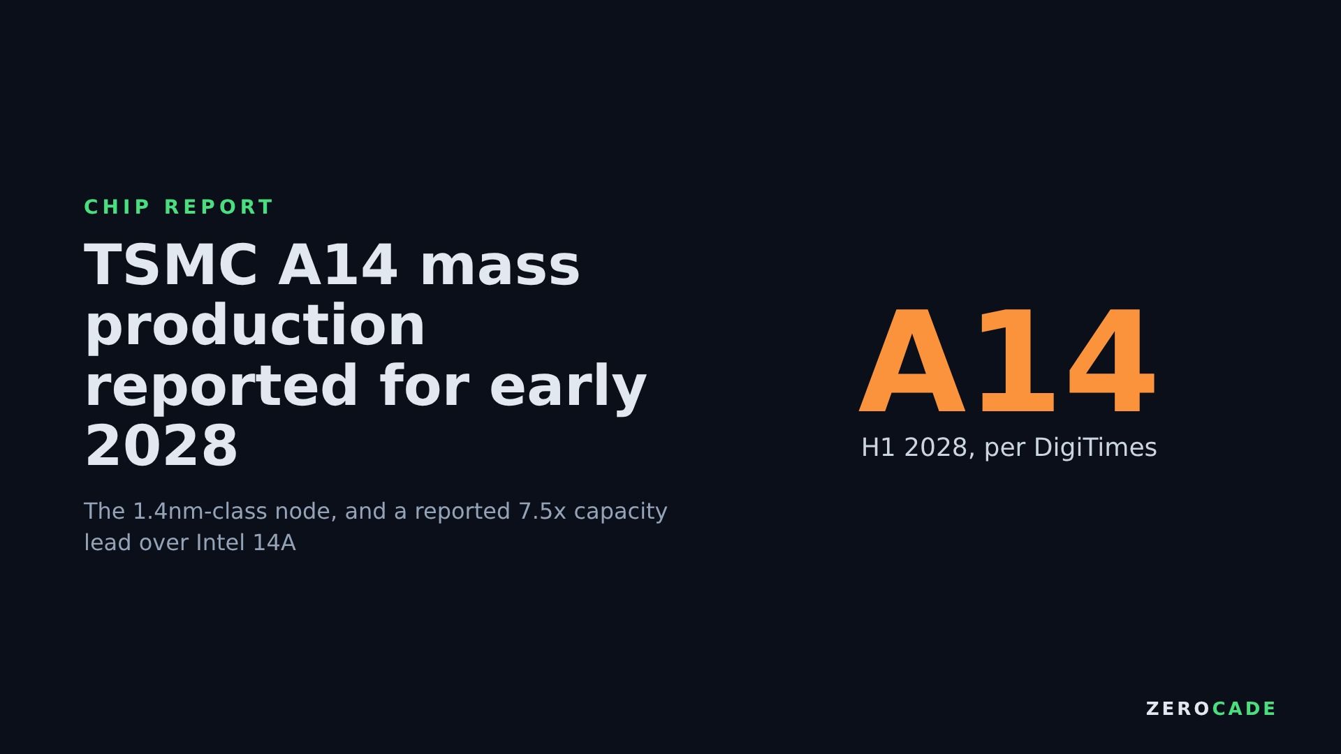
- Taiwan's DigiTimes reports that TSMC's A14 process, its next step after 2nm, will enter mass production in the first half of 2028. Risk production is reported for late 2027. TSMC hasn't confirmed the dates itself.
- The same report says TSMC's A14 capacity in 2028 will be 7.5 times that of Intel 14A, Intel's rival node for the same year.
- TSMC's earlier figures for A14 over N2: up to 15% faster at the same power, up to 30% less power at the same speed, and up to 20% more density.
- No chips have been announced on A14 yet. Apple is widely expected to be an early customer, but that's speculation for now.
What the report says
The news comes from DigiTimes, a Taiwanese trade publication with good supply-chain sources, relayed by Wccftech on October 29, 2026. According to the report, A14 moves to mass production in the first half of 2028. That's when TSMC starts making customer chips in volume, after a risk-production phase where early designs are tested on the line.
The headline number is capacity. DigiTimes says that in 2028, TSMC's A14 capacity will be 7.5 times Intel's 14A capacity. The report, as relayed, doesn't say exactly how that's measured. It's most likely wafer output, but treat the exact unit as unconfirmed. Two TSMC fabs are said to lead the ramp: Fab 20 at Baoshan in Hsinchu and Fab 25 in central Taiwan.
DigiTimes has a decent track record on TSMC capacity and timing, but this is still a report, not a TSMC announcement. TSMC's own A14 page only says development is "progressing smoothly with yield performance ahead of schedule".
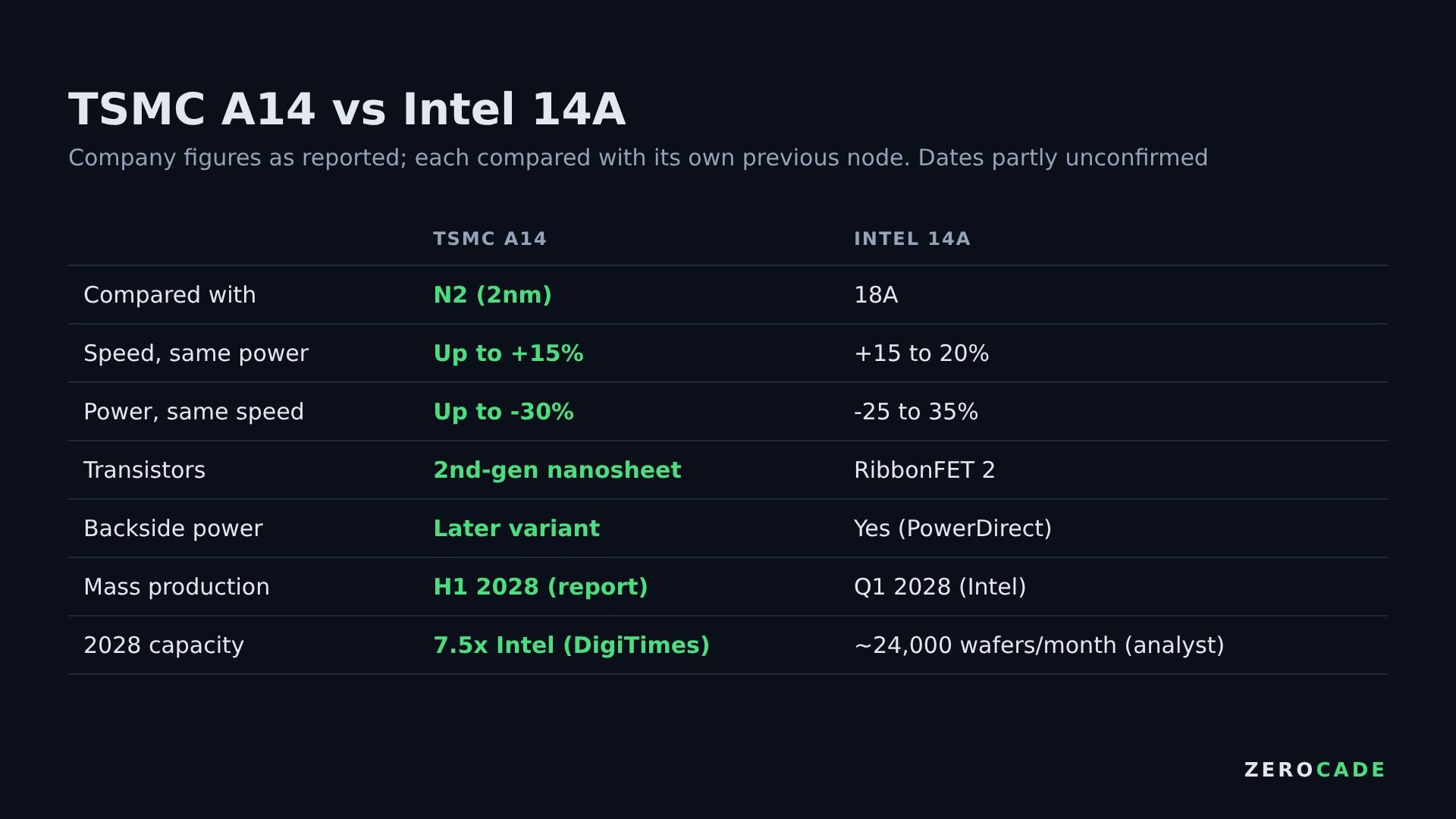 Image: Zerocade
What A14 improves over 2nm
A14 is TSMC's "1.4nm-class" node. The name is a label for a new generation, not a measurement of any part of the chip. Our process node explainer covers why.
TSMC's figures for A14 over its N2 (2nm) process, which started volume production in late 2025, are:
- Up to 15% more speed at the same power. Some later summaries quote a 10 to 15% range.
- Up to 30% less power at the same speed.
- Up to 20% more logic density, so more transistors fit in the same area.
It uses second-generation nanosheet transistors, where the gate wraps fully around stacked silicon sheets to control current better. It also brings a new cell library TSMC calls NanoFlex Pro, which lets chip designers mix fast and power-saving building blocks on the same chip. According to Wccftech's summary, the base A14 delivers power from the front of the chip. A later variant is expected to add backside power, the trick of moving power wiring under the transistors that TSMC's A16 introduces first.
 Image: TSMC
How Intel 14A compares
Intel's 14A is its answer, aimed at the same 2028 window. Intel told Wccftech in September that volume production will begin in Q1 2028, with risk production for its own products in 2027. It uses Intel's second-generation RibbonFET transistors, PowerDirect backside power, and the newest High-NA EUV lithography machines. TSMC is sticking with standard EUV for A14.
On paper, 14A is technically ambitious. The gap is scale and customers. Analyst Jeff Pu of GF Securities projected Intel's 14A output at around 24,000 wafers a month in 2028. Analysts at Piper Sandler say companies including Apple, AMD, Nvidia, Qualcomm, Google, Microsoft, Tesla and Amazon are evaluating 14A, but there's no confirmed big outside customer yet. Intel has said it needs outside customers to justify building 14A at scale.
That's why a 7.5x capacity gap, if accurate, matters. Chip designers need a guarantee they can get enough wafers. TSMC is already reported to be sold out for leading-edge capacity through 2028.
When it reaches your devices
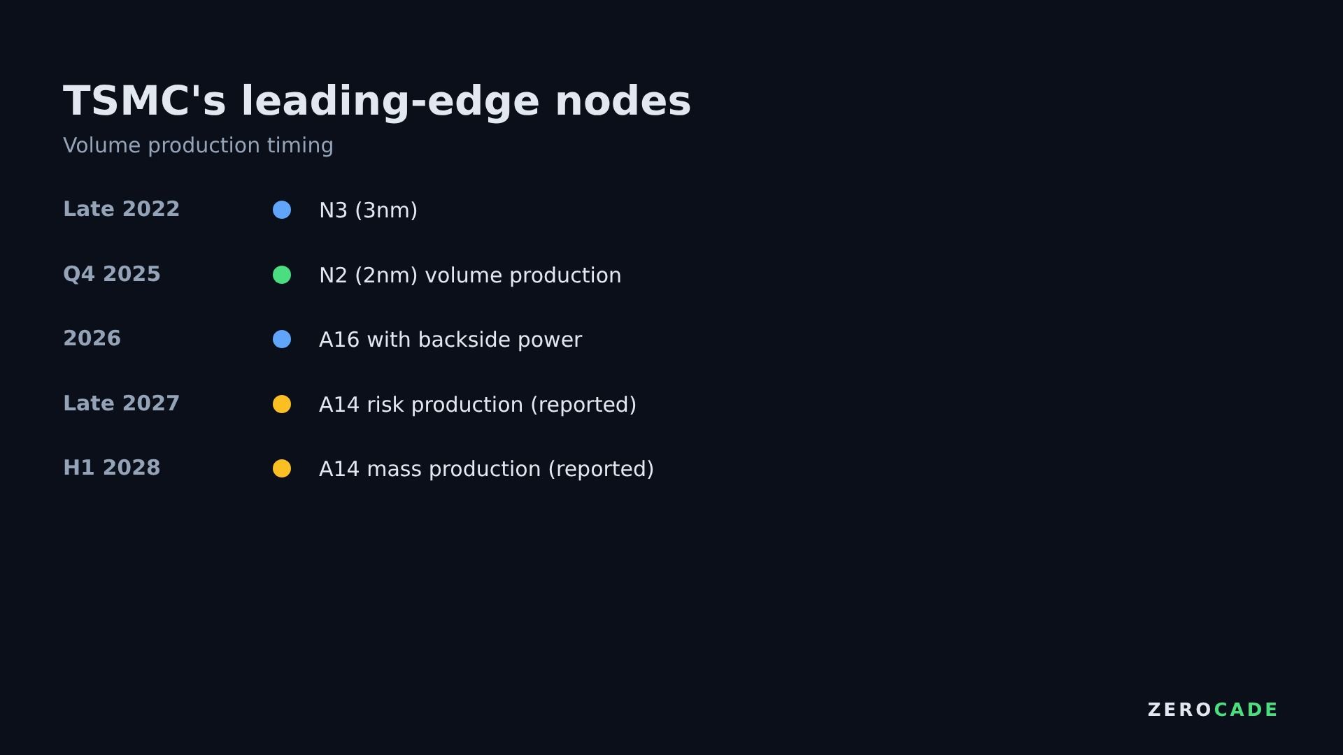 Image: Zerocade
If the 2028 timing holds, the first A14 chips would most likely be phone processors, as with every recent TSMC node. Apple usually gets first access, so an iPhone chip in late 2028 is the common guess. Laptop and desktop chips from AMD, Apple and possibly Nvidia would follow. A next-generation console APU on A14 is possible but nothing has been said about that.
For Indian buyers, none of this changes prices today. Leading-edge wafers keep getting more expensive with each node, so the first A14 phones and laptops will almost certainly be premium products.
Watch for TSMC's own update. It usually shares node timelines at its Technology Symposium in April, and ETNews reports TSMC will publish A14 memory-cell research by the end of this year.